 Analysis and Function Elucidation of Fine Clusters and Defects in Materials Invisible by Electron Microscopy
update:2021/07/07
- Features and Uniqueness
-
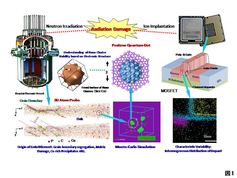
- It is well known that nano-scale impurity/solute clusters, defects, defect clusters and their complexes affect the mechanical and electrical properties in materials. However, it is very difficult to observe these objects even by state-of-the-art electron microscopes. We overcome the difficulty by employing noble two techniques: laser three-dimensional atom probe (3D-AP) technique and positron annihilation spectroscopy (PAS). Laser 3D-AP can map out each atom in various materials (metals, semiconductors, insulators) in three-dimensional real space with nearly atomic scale resolution. PAS can detect vacancy-type defects and defect-impurity complexes very sensitively.
- Practical Application
-
By combining these methods, we are going to reveal the functions of the fine impurity clusters and defects to the materials: developments of new nano-structured materials, the mechanism of degradation of aged structural materials, the fall in the yield of semiconductor device production, and developments of quantum devices etc.
- Keywords


 Medical
 Life Sciences
 Information Communication
 Nanotechnology / Materials
 Energy
 Manufacturing Technology
 Social Infrastructure
 Frontier
 Liberal Arts


