 Nano-Scale Total-Analysis Based on TEM
update:2020/06/16
- Features and Uniqueness
-
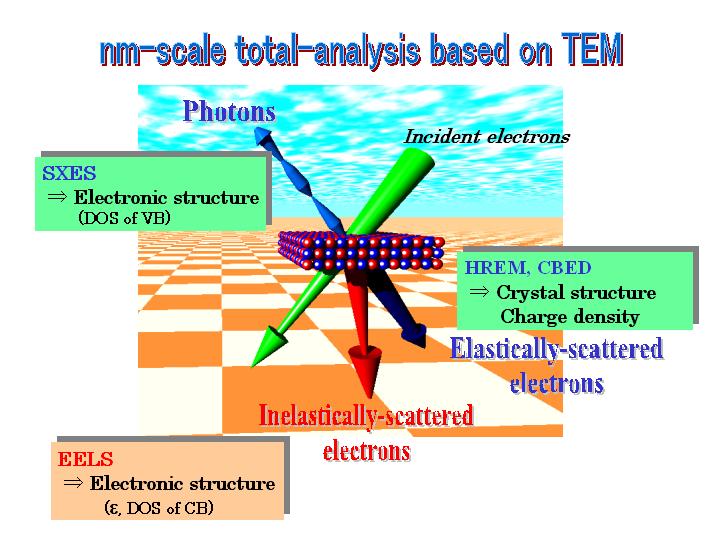
- Our lab develops accurate nanometer scale characterization methods of crystal structures by convergent-beam electron diffraction (<strong>CBED</strong>) and electronic structures by electron energy-loss spectroscopy (EELS) and soft-X-ray emission spectroscopy (<strong>SXES</strong>) for evaluating new functional materials. For performing crystal structure studies, we developed a new Ω-filter electron microscope and a refinement soft-ware, which can perform not only atom positions but also electrostatic potential and charge distributions. For electronic structure studies, a high-resolution EELS microscope and SXES instruments were developed.
- Practical Application
-
Collaborated research of Local structures (symmetry, polarity, lattice defects) by CBED and electronic structures (bandgap, dielectric property and chemical state) by EELS and SXES on semiconductors, metals and dielectric materials are acceptable. Instructions of those analysis methods are also acceptable.
- Keywords
Researchers
Institute of Multidisciplinary Research for Advanced Materials
Masami Terauchi, Professor
Doctor of Science


 Medical
 Life Sciences
 Information Communication
 Nanotechnology / Materials
 Energy
 Manufacturing Technology
 Social Infrastructure
 Frontier
 Liberal Arts


