
 Medical
 Life Sciences
 Information Communication
 Environment
 Energy
 Manufacturing Technology
 Social Infrastructure
 Frontier
 Human and social sciences

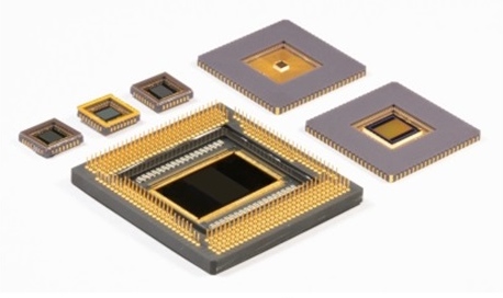
 Development of Advanced Device and Process Technologies and New Image Sensors
- Features and Uniqueness
-
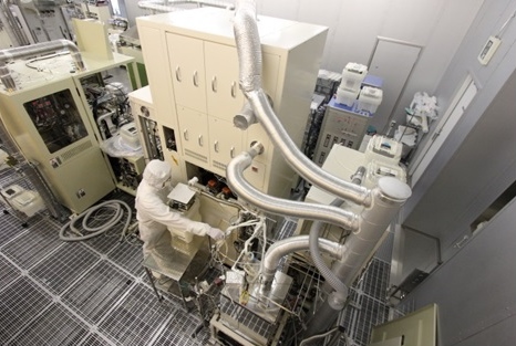
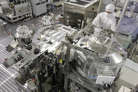
Toward the ultimate performances of image sensors, advanced research activities are being conducted that cover a wide range of technology fields from cleanroom infrastructure, materials, process equipment, process, device, circuit, assembly, signal processing, measurement/evaluation and reliability. Following technologies have been successfully commercialized:
A fast and accurate measurement technology of electrical characteristics for over 1 million transistors
A wide dynamic range CMOS image sensor technology capturing images over five decade brightness ranges
An ultra-fast CMOS image sensor technology with 10 million frames/sec - Practical Application
-
Followings are available for industry collaborators:
A. 200mm-diameter-wafer silicon device fabrication utilizing the ultra-clean facility including wafer mutual fabrication processing between device manufacturers.
B. Process technology development and various kinds of analyses.
C. Development of new image sensors. - Keywords
