
 Medical
 Life Sciences
 Information Communication
 Environment
 Energy
 Manufacturing Technology
 Social Infrastructure
 Frontier
 Human and social sciences

 Hands-On Access Fabrication Facility –Open Facility for MEMS and Semiconductor Prototyping–
- Overview of Technology
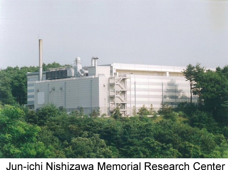
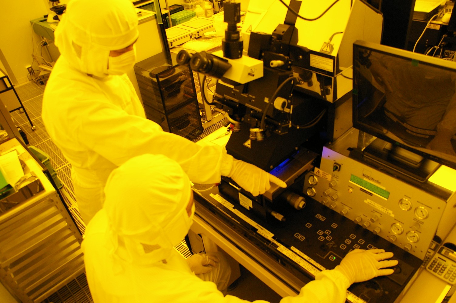
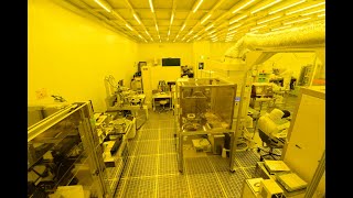
We offer shared facility for the development of semiconductor prototypes equipped with 4-inch, 6-inch and some 8-inch wafer fabrication tools available on an hourly basis. Know-how accumulated at Tohoku University is available, and staff provide maximum support for prototyping. The service is performed at the 1,200 m2 Super Clean Room on the second floor of the Junichi Nishizawa Memorial Research Centre at Tohoku University. For information on equipment and fees, see our website.
- Comparison with Conventional Technology
More than 10 experienced technical staff assist customer's usages. Standard process conditions for each process, such as etching and deposition, are provided. allowing customers to start prototyping immediately. Various materials other than silicon can also be supported.
- Features and Uniqueness
-
We support the development of devices and semiconductor materials such as MEMS, optical elements and RF components.
Technical consultation on devices and processes before and during prototyping is also available.
A
'Prototype lab' for device packaging is also available.
The museums where you can learn about the history of semiconductors, measuring instruments and sensors are open.
As part of Technology Co-creation for Semiconductor of Tohoku University, we promote R&D of semiconductors and the development of human resources.
On-demand semiconductor human resource development programs for students and engineers are available.
As a member of the MEXT's Advanced Research Infrastructure for Materials (ARIM) program, we are involved in sharing facility and data. - Practical Application
-
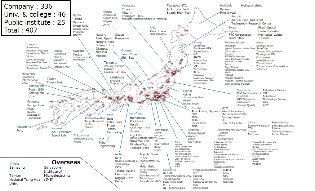
More than 330 companies have used our shared facility since its launch in 2010, not only from device manufacturers such as MEMS, but also from manufacturers of materials, mechanical components and equipment. To date, we have successfully supported the commercialization of about 10 devices.
- Keywords
Researchers
Micro System Integration Center
Kentaro Totsu, Professor
Doctor of Engineering
