"S" Researcher - 9 Result(s)

S

 S

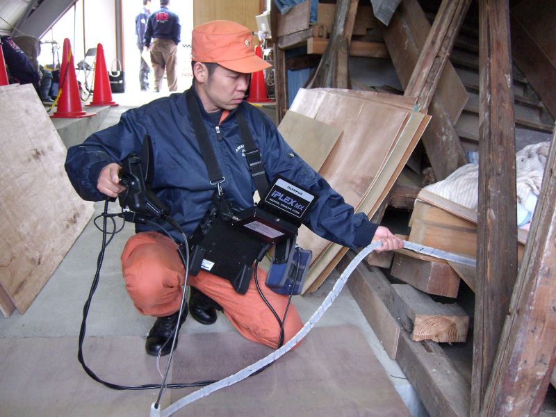
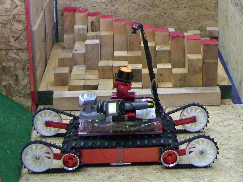
Robot Technology for Achieving Secure Society

NEXT
PREV
特徴・独自性
  • Tadokoro Laboratory developed ‘Active Scope Camera,' a world-unique rescue robot that can search deep in rubble piles of collapsed structures through a gap of a few cm wide. It also developed ‘Quince,' a world-unique unmanned ground vehicle that could survey the second to fifth floors of Nuclear Reactor Buildings of Fukushima-Daiichi Nuclear Power Plant. Its technologies was applied industries, including unmanned transfer vehicle for outdoors under ice and snow environment being actually used in a factory of Toyota Motor East Japan, and ‘Robo-Scope' for debris inspection in collaboration with Shimizu Corporation.
実用化イメージ

We have a policy of education through and research for solution to actual problems. Current nearly ten collaborative researches focuses on outdoor investigation, infrastructure/plant inspection, and remote/autonomous task execution by robots.

Researchers

Graduate School of Information Sciences

Satoshi Tadokoro

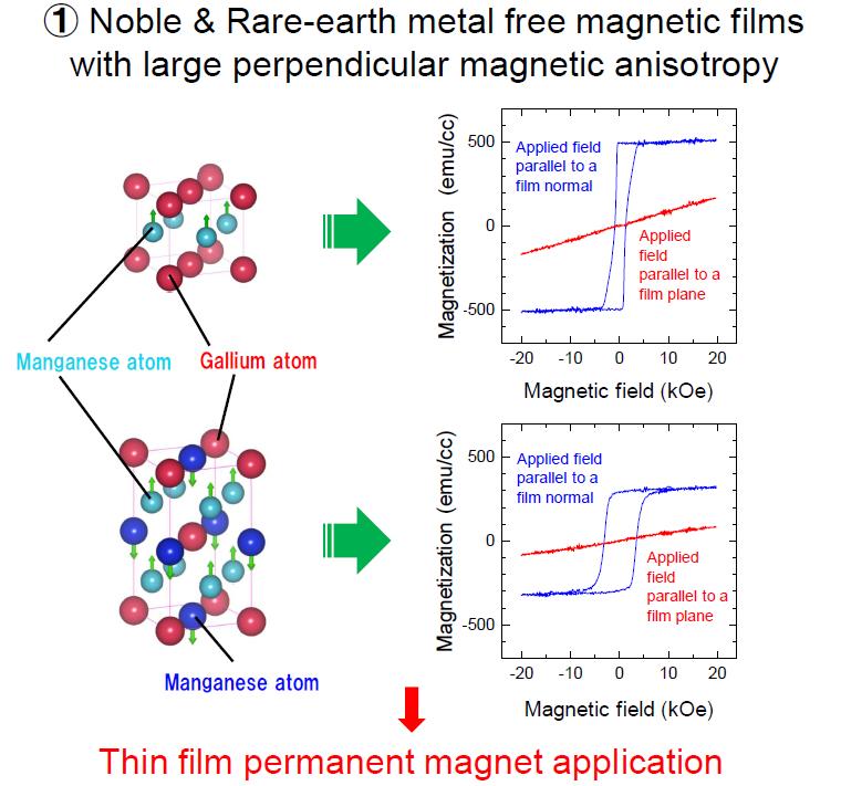
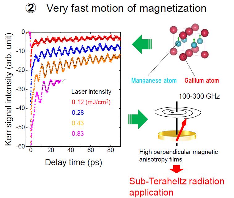
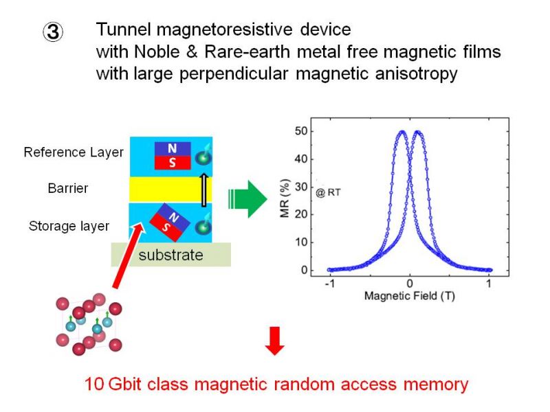
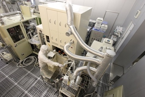
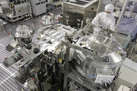
Spintronics Devices and Materials

NEXT
PREV
特徴・独自性
  • Spintronics is a technology utilizing electron spin which provided magnetic sensor, nonvolatile magnetic memory, and so on. Our studies are as below.
  • Noble & Rare-earth free magnetic films with large perpendicular magnetic anisotropy. We achieved to develop various Mn-bases alloy films exhibiting high perpendicular magnetic anisotropy (Fig.1 ).
  • THz range observation of magnetization motion. We achieved to detect a motion of magnetization using pulse laser in time domain (Fig. 2).
  • Novel organic spin devices. We achieved to fabricate hybrid junction consisting of an organic layer sandwiched by two inorganic magnetic layers and to observe magnetoresistance effect.
  • Tunnel Magnetoresistive devices: We are developing TMR devices with Mn-Ga alloys films (Fig.3 ).
実用化イメージ

Magnetic memory and storage. Microwave and Terahertz wave. Magnetic sensors.
We hope to conduct collaborative research with a willing company for a practical application of these devices and materials in industry.

Researchers

Advanced Institute for Materials Research

Shigemi Mizukami

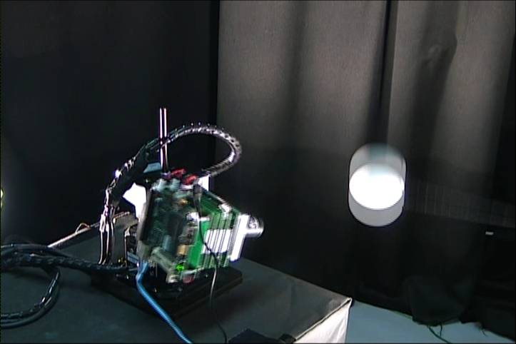
Development of Advanced Device and Process Technologies and New Image Sensors

NEXT
PREV
特徴・独自性
  • Toward the ultimate performances of image sensors, advanced research activities are being conducted that cover a wide range of technology fields from cleanroom infrastructure, materials, process equipment, process, device, circuit, assembly, signal processing, measurement/evaluation and reliability. Following technologies have been successfully commercialized:
  • A fast and accurate measurement technology of electrical characteristics for over 1 million transistors
  • A wide dynamic range CMOS image sensor technology capturing images over five decade brightness ranges
  • An ultra-fast CMOS image sensor technology with 10 million frames/sec
実用化イメージ

Followings are available for industry collaborators:
A. 200mm-diameter-wafer silicon device fabrication utilizing the ultra-clean facility including wafer mutual fabrication processing between device manufacturers.
B. Process technology development and various kinds of analyses.
C. Development of new image sensors.

Researchers

New Industry Creation Hatchery Center

Shigetoshi Sugawa

Imaging and photoregulation of biological functions

特徴・独自性
  • To properly understand the functions of biomolecules, it is essential to observe them under physiological conditions where the interactions with other biomolecules are preserved. Therefore, we are developing new functional molecules using both organic chemistry and protein science approaches, and working on the visualization and optical control of biomolecules and their functions. Especially, we have developed fluorescent probes that quantitate the concentration of biomolecules or ions in subcellular regions such as organelles and caged compounds and photoswitches that optically manipulate the biomolecular functions.
実用化イメージ

Researchers

Institute of Multidisciplinary Research for Advanced Materials

Shin Mizukami

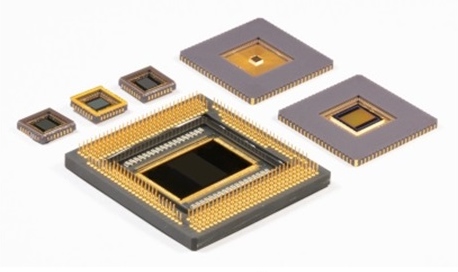
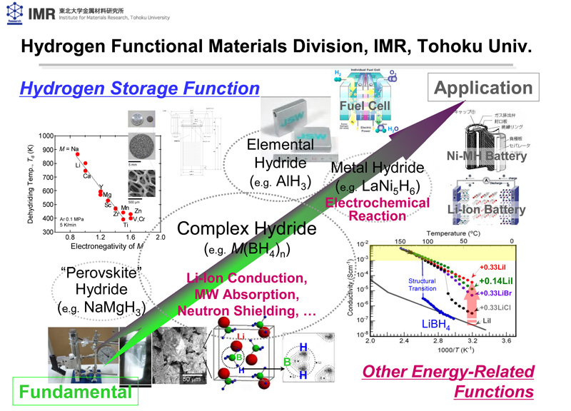
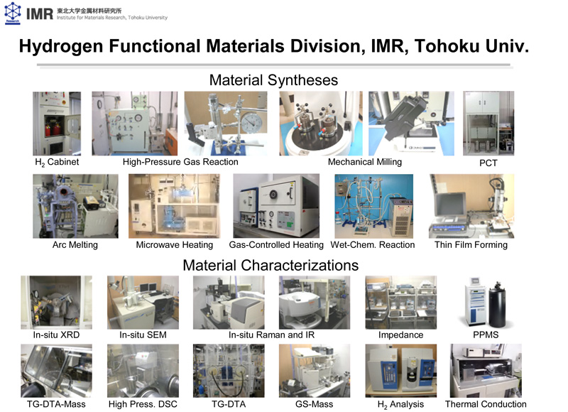
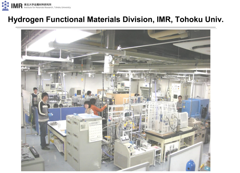
“HYDRIDE" Researches for Energy Applications

NEXT
PREV
特徴・独自性
  • This group is engaged in basic and applied researches of "hydrides" for practical use in hydrogen energy system. The main subject is the exploration of advanced hydrogen storage materials which support hydrogen energy technologies such as fuel cells. Currently, we synthesize a wide variety of novel hydrides composed of lightweight metals with specific nano-structures using advanced techniques for crystal and electronic structure analyses. In addition to the hydrogen storage, we develop the wide research fields related to hydrides, such as fast lithium ionic conductors.
実用化イメージ

Besides the contributions in industrial progress through the material development for future hydrogen energy system and next-generation secondary battery, we positively provide technical assistance to organizations and companies concerned about our findings.

Researchers

Advanced Institute for Materials Research

Shin-Ichi Orimo

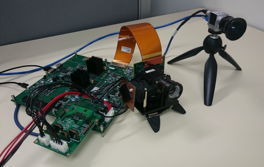
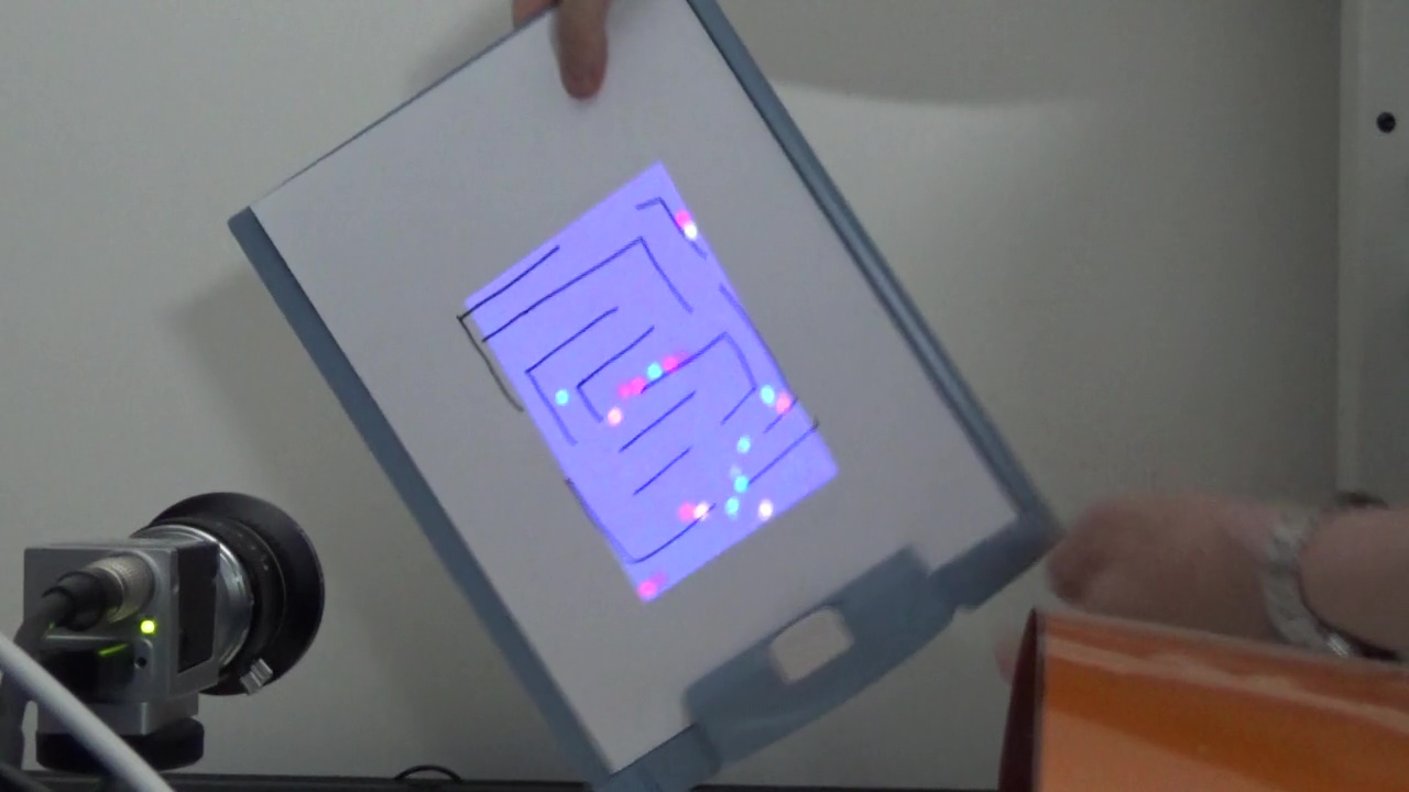
High-Speed Vision for Real-Time Motion Analysis

NEXT
PREV
特徴・独自性
  • We are investigating high-speed vision systems that enable real-time image acquisition and visual processing at frame rates substantially higher than the standard video rate.
実用化イメージ

High-speed vision systems are useful for fast measurement and control of dynamic systems in general. When combined with external facilities such as high-speed projectors or acceleration sensors, they enable further wider applications including fast 3D measurement or object identification.

Researchers

Unprecedented-scale Data Analytics Center

Shingo Kagami

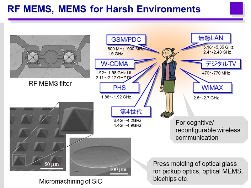
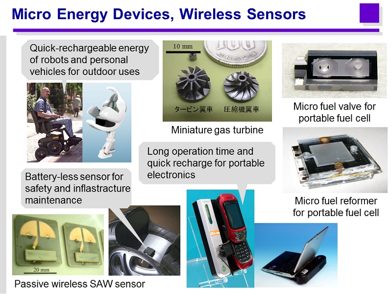
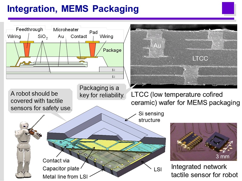
MEMS/Micromachines and Microfabrication Technology

NEXT
PREV
特徴・独自性
  • We are studying MEMS (Micro Electro Mechanical Systems) and related technologies, which are typically used for the input/output of information/communication devices, the safety of automobiles etc. Our representative topics include integrated sensors, piezoelectric devices, RF MEMS, micro energy devices and wafer-level packages. Our facilities are open-accessible and well equipped with a lot of tools for lithography, dry/wet etching, thin film deposition, wafer bonding, device mounting and evaluations, which can be operated by each researcher. Using these tools, a variety of MEMS are being prototyped. Also, new microfabrication tools are being developed by ourselves.
実用化イメージ

We are collaborating with many companies, from which visiting researchers are dispatched to our laboratory. We also accept companies which want to just use specific tools in our facilities. Consultation is always welcome.

Researchers

Graduate School of Engineering

Shuji Tanaka
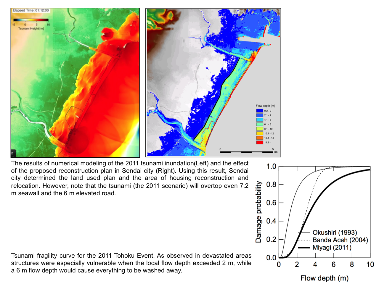
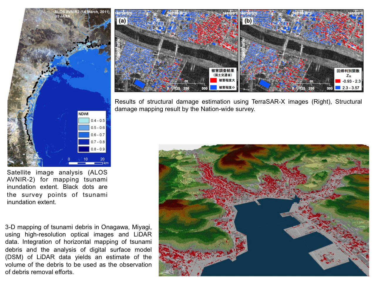
Spintronics device

特徴・独自性
  • To realize ultralow-power and high-performance integrated circuit and information processing, spintronics physics, material, devices are studied.
実用化イメージ

Researchers

Research Institute of Electrical Communication

Shunsuke Fukami