Medical
 Life Sciences
 Information Communication
 Environment
 Nanotechnology / Materials
 Energy
 Manufacturing Technology
 Social Infrastructure
 Frontier
 Human and social sciences

"S" Keywords - 146 Result(s)
S
[self]
Brain Mechanism Realizing Human Mind
ResearchersInstitute of Development, Aging and Cancer Motoaki Sugiura
|
[self-driving car]
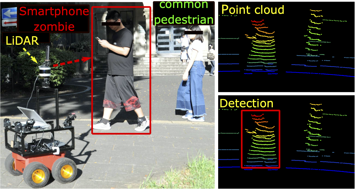
Coexistence of humans and mobile robots
ResearchersGraduate School of Engineering Yusuke Tamura
|
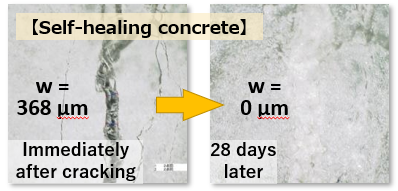
[self-healing concrete]
Development of functional concrete
ResearchersGraduate School of Engineering Tomoya Nishiwaki
|
[Semiconductor]
Electronic properties of nanostructures and nanodevices
ResearchersAdvanced Institute for Materials Research Tomohiro Otsuka
|
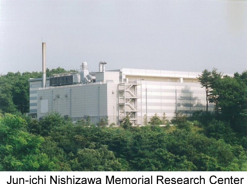
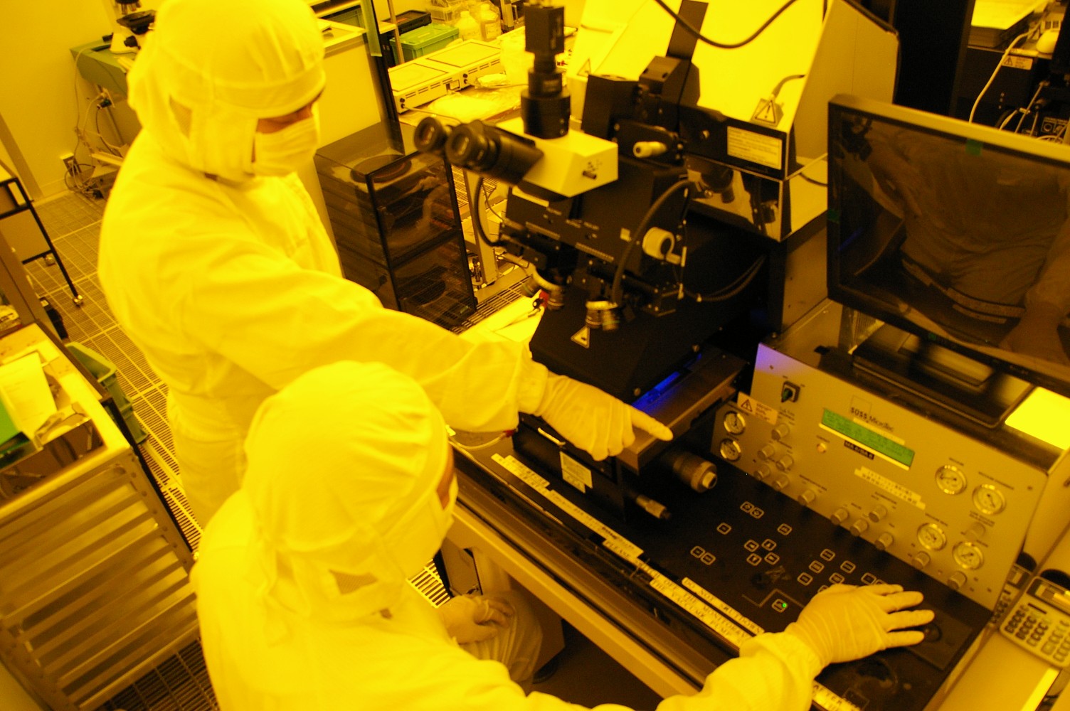
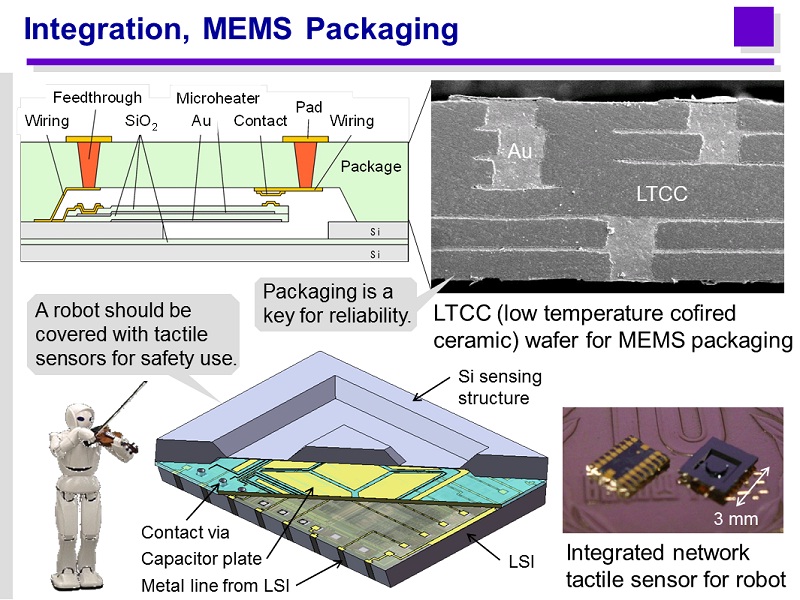
Hands-On Access Fabrication Facility –Open Facility for MEMS and Semiconductor Prototyping–
ResearchersMicro System Integration Center Kentaro Totsu
|
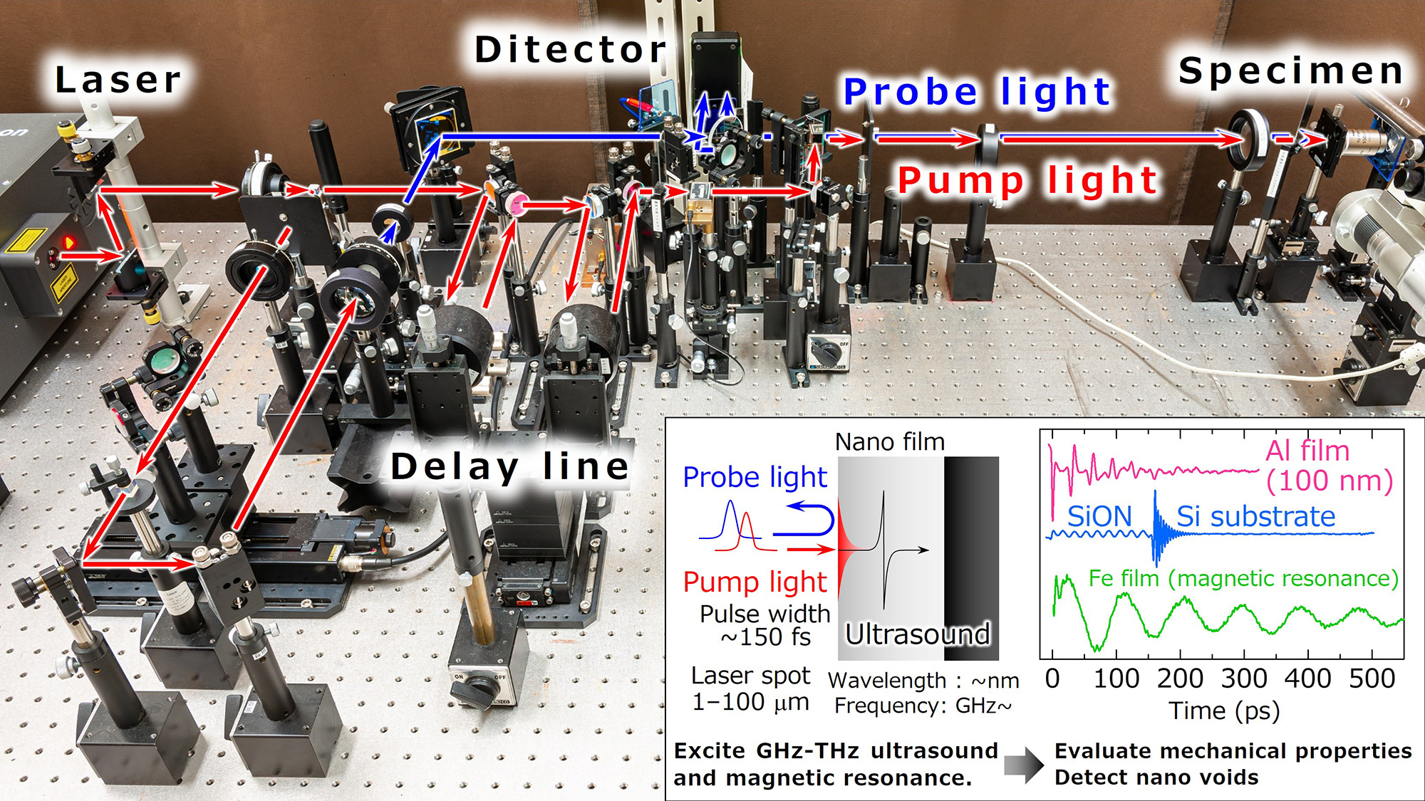
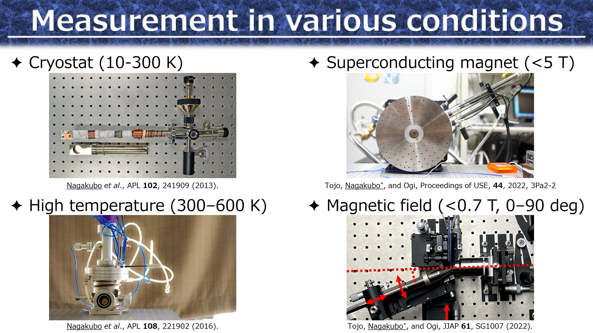
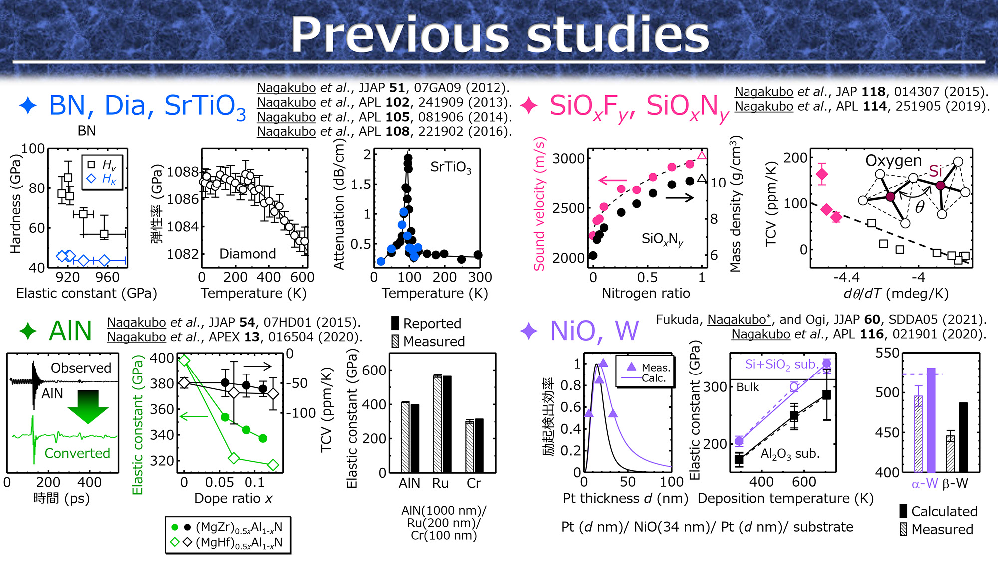
Mechanical and acoustic properties of nm devices studied by GHz-THz ultrasonics
ResearchersGraduate School of Engineering Akira Nagakubo
|
[Semiconductor Integrated Circuit]
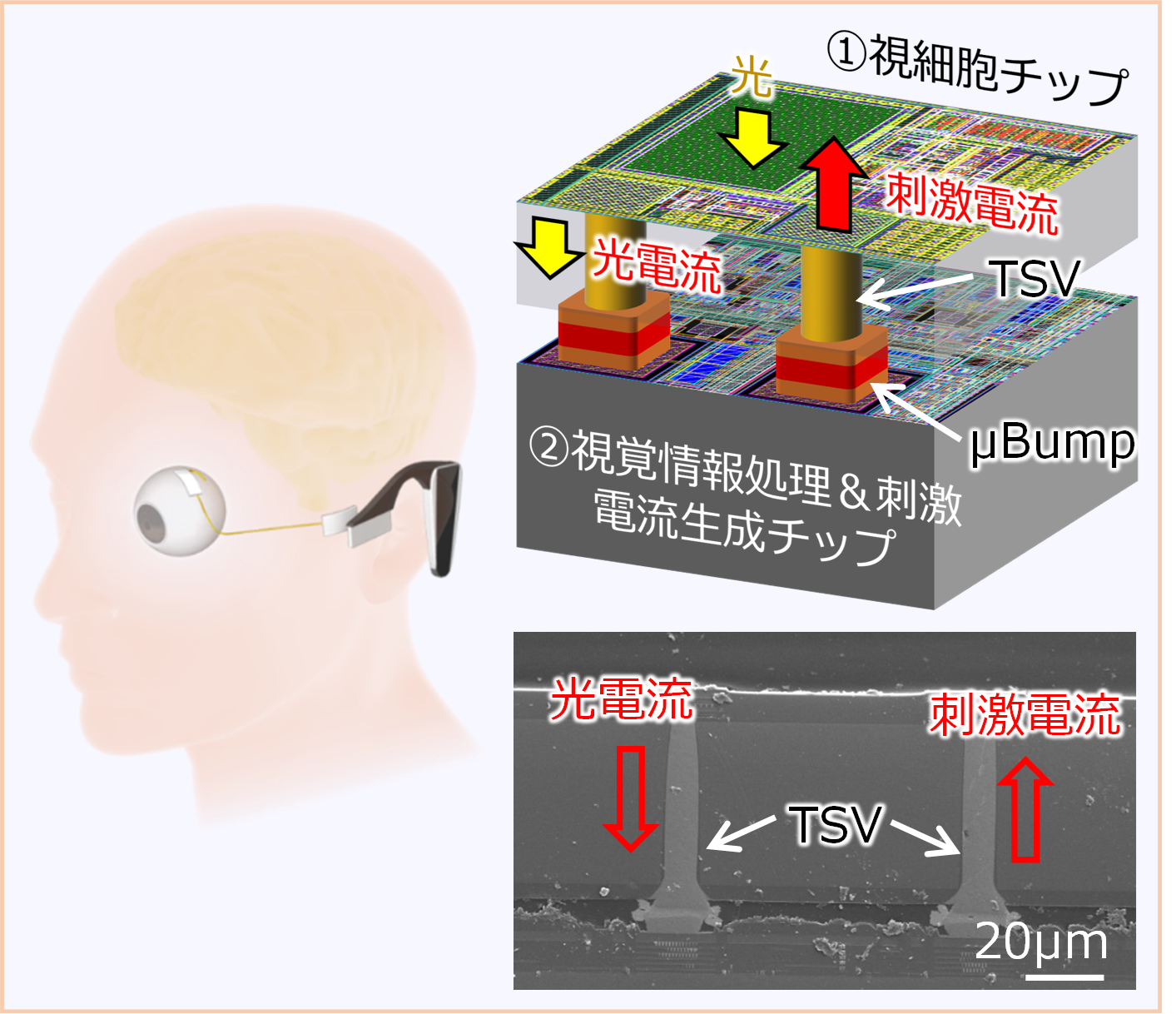
Development of Biomedical Micro/Nano Integrated System Using LSI Technology
ResearchersGraduate School of Biomedical Engineering Tetsu Tanaka
|
[Semiconductor processing]
Development of Advanced Device and Process Technologies and New Image Sensors
ResearchersNew Industry Creation Hatchery Center Shigetoshi Sugawa
|
[Sensor]
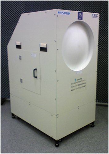
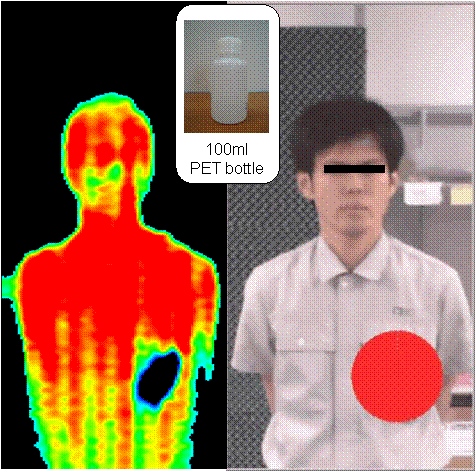
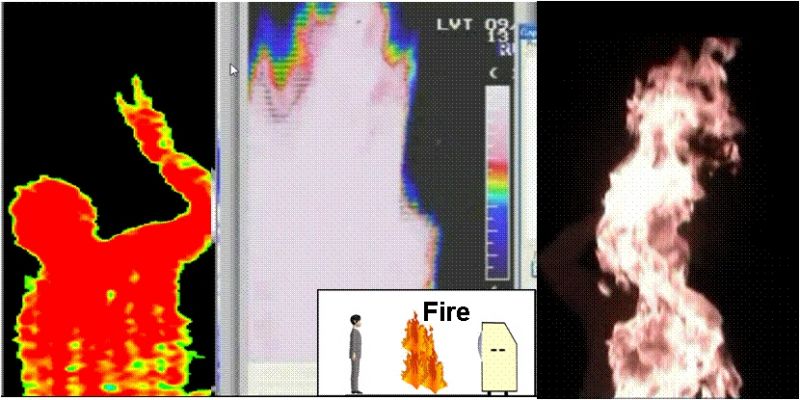
Development of Passive Millimeter-wave Imaging Device for Practical Applications
ResearchersGraduate School of Engineering Hiroyasu Sato
|
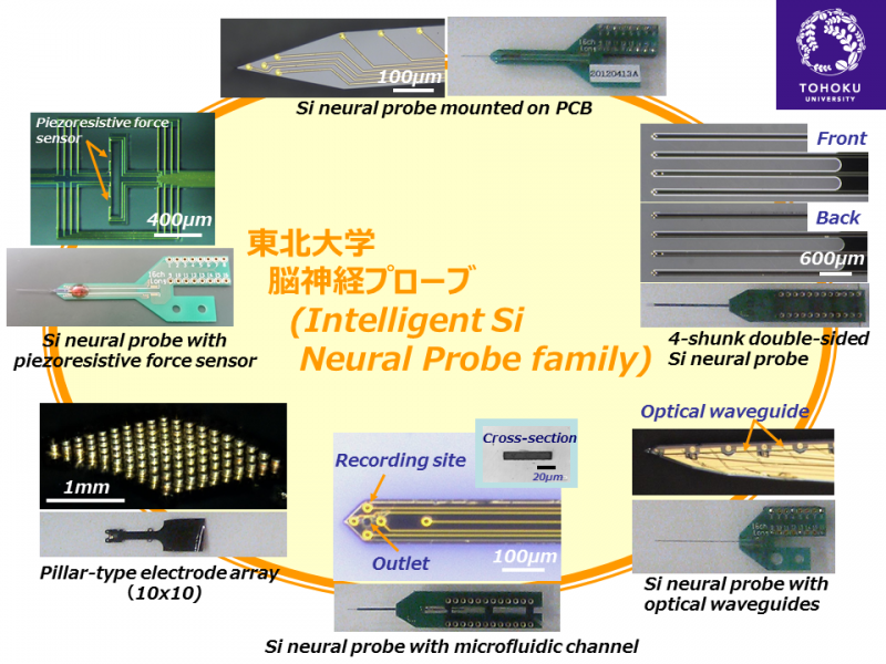
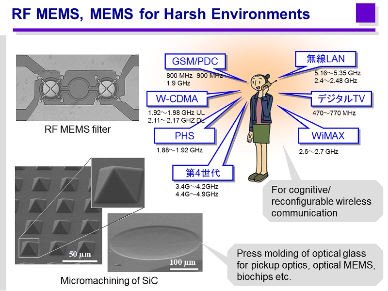
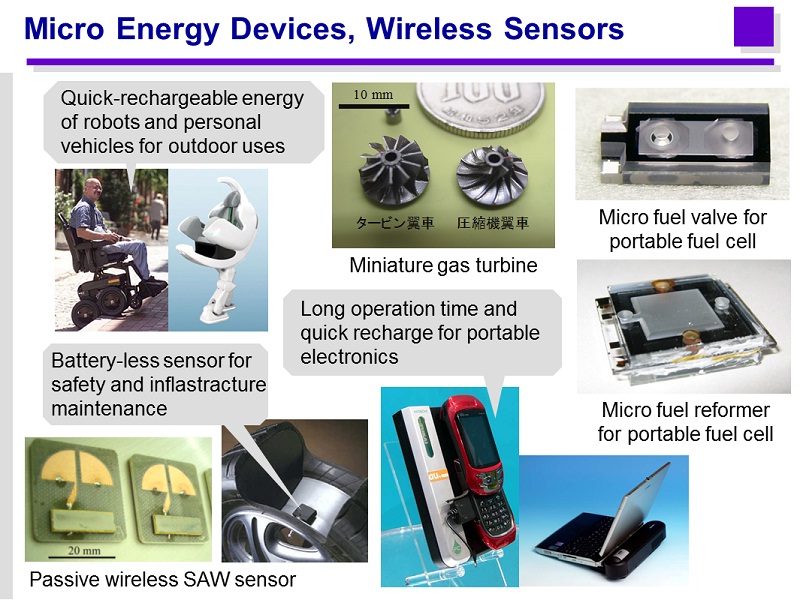
MEMS/Micromachines and Microfabrication Technology
ResearchersGraduate School of Engineering Shuji Tanaka
|
Hands-On Access Fabrication Facility –Open Facility for MEMS and Semiconductor Prototyping–
ResearchersMicro System Integration Center Kentaro Totsu
|
[Service Engineering]
Data Analytics for Creation of Social Values
ResearchersGraduate School of Economics and Management Tsukasa Ishigaki
|
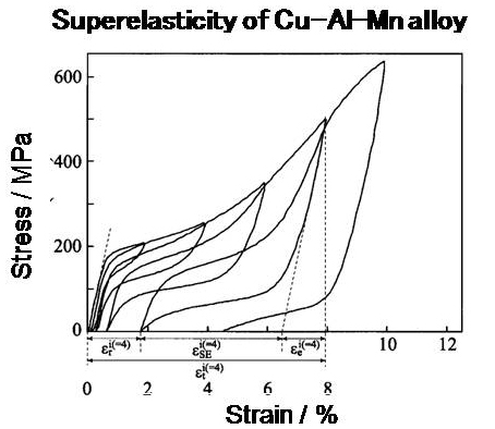
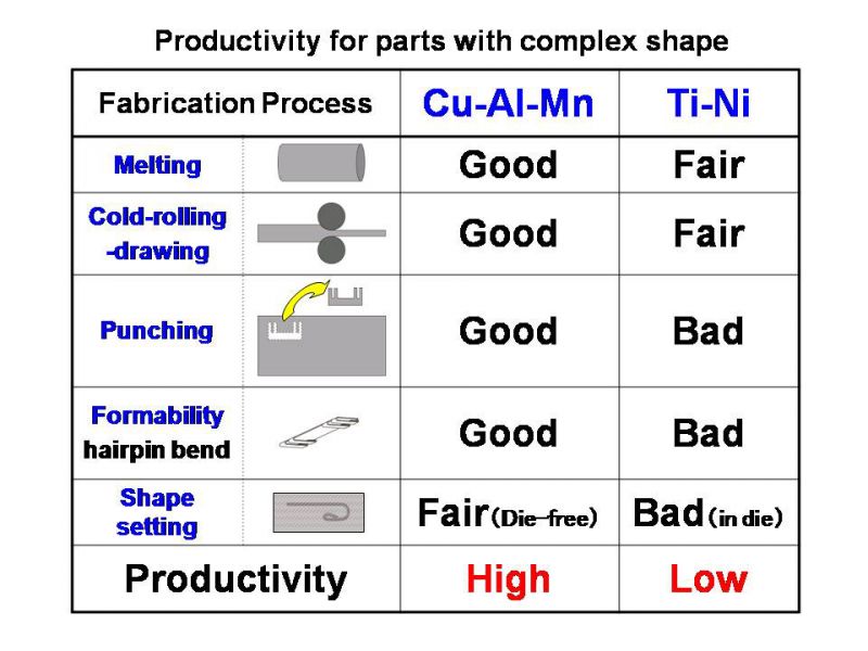
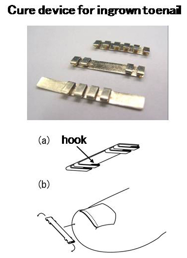
[Shape memory alloy]
Novel Cu-Based Shape Memory Alloy with High Ductility
ResearchersGraduate School of Engineering Ryosuke Kainuma
|
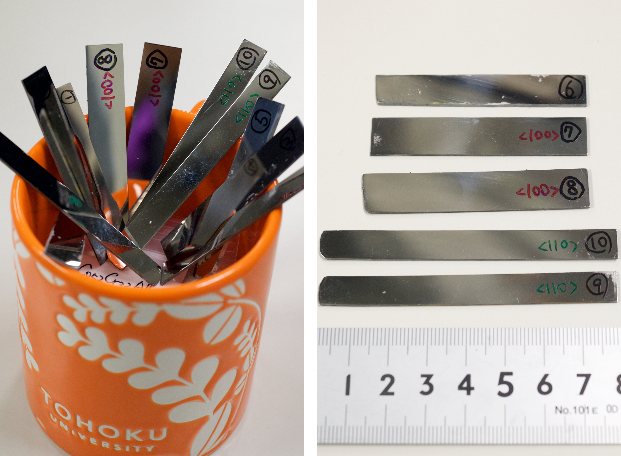
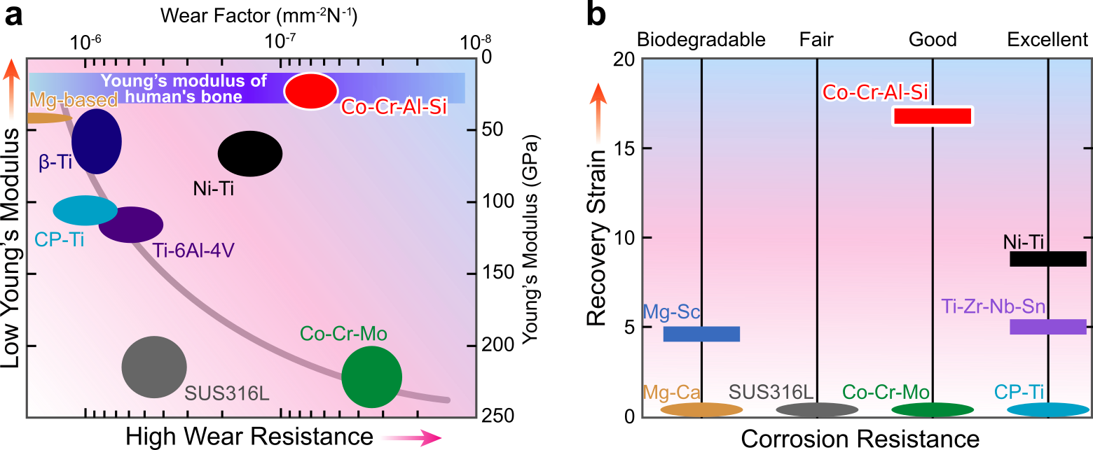
Novel CoCr-based superelastic metallic biomaterial with low Young's modulus
ResearchersGraduate School of Engineering Xiao Xu
|
[Si semiconductors]
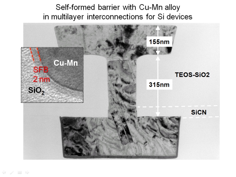
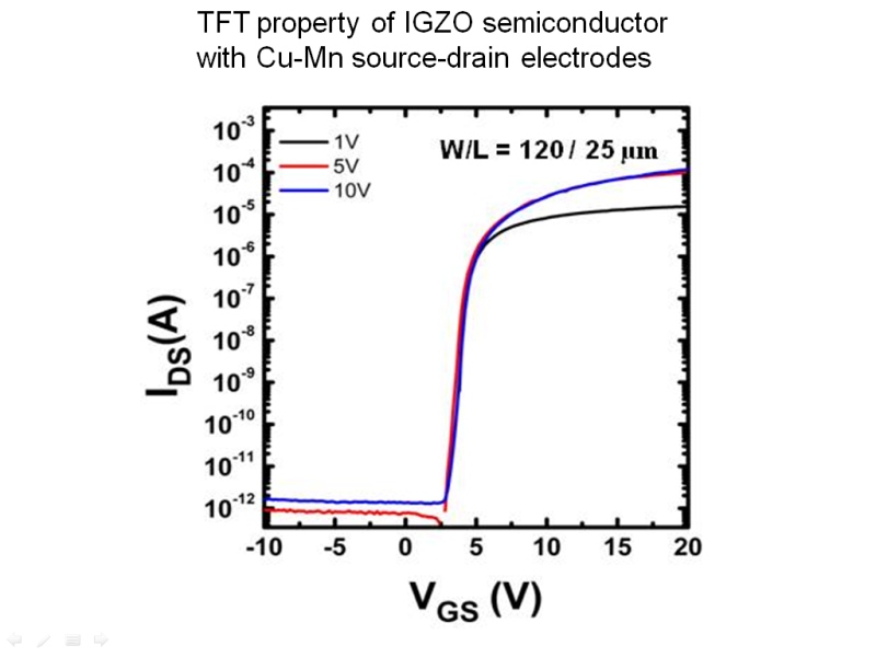
Development of Interconnect Materials and Processes for High Performance and High Reliability Electric Devices
ResearchersNew Industry Creation Hatchery Center Junichi Koike
|
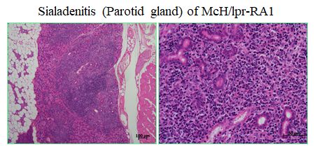
[Sialadenitis]
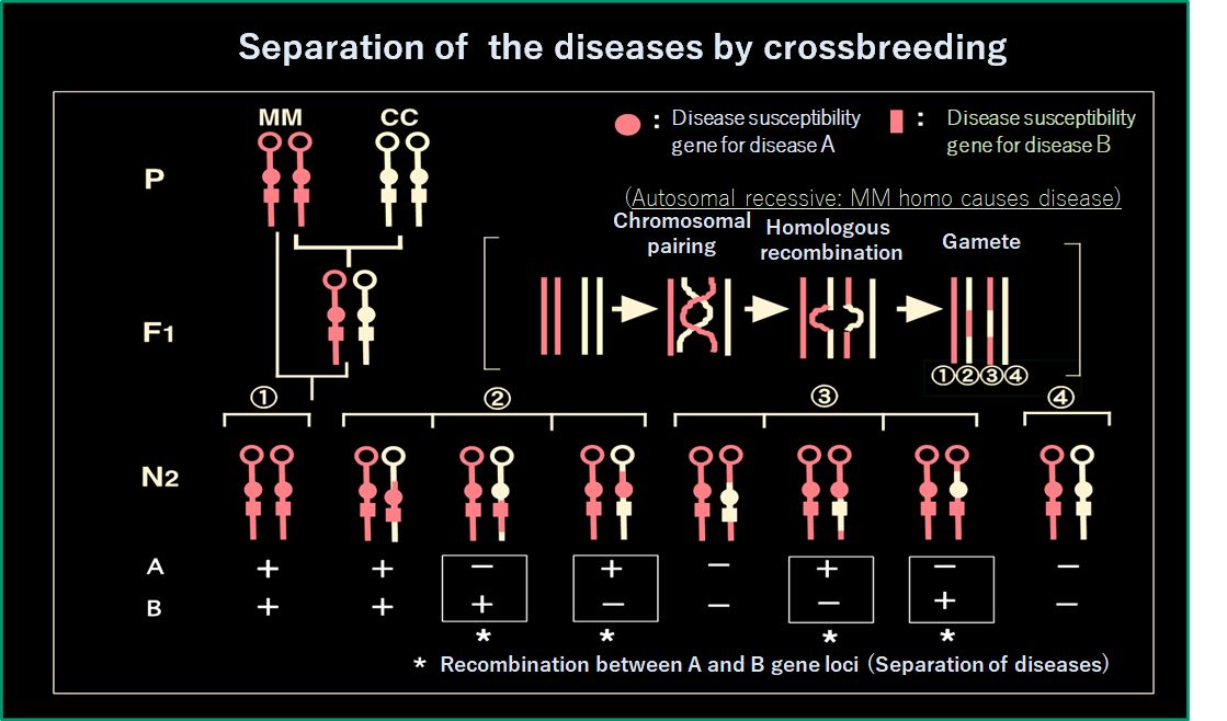
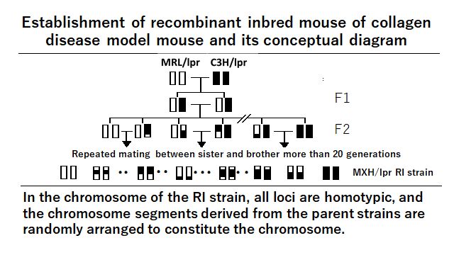
Development of Recombinant Inbred Mice with a Genetic Predisposition to Collagen Disease
ResearchersGraduate School of Biomedical Engineering Tetsuya Kodama
|
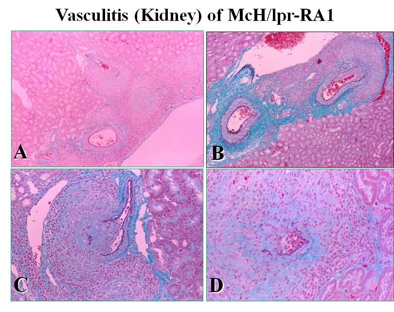
Development of McH-lpr/lpr-RA1 mouse, a study model that spontaneously develops severe autoimmune arthritis, vasculitis, and sialadenitis
ResearchersGraduate School of Biomedical Engineering Tetsuya Kodama
|
[SiC power devices]
Development of Interconnect Materials and Processes for High Performance and High Reliability Electric Devices
ResearchersNew Industry Creation Hatchery Center Junichi Koike
|
[Side-Channel Attack]
Visual Computing with Secure ICT in the Big Data Era
ResearchersAdministrative Staff Takafumi Aoki
|
[Signal processing]
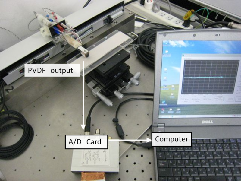
Study on Tactile/Touch Feeling Sensor
ResearchersGraduate School of Biomedical Engineering Mami Tanaka
|